Over the course of many years that the author of this article mingled with electronics,
firstly as an amateur and then as a professional, probably the most frequent request
from friends and relatives was to build a small battery charger.
It is truth that since the worldwide introduction of Li-ION technology old-faithful Nickel based accumulators have lost a considerable percentage of uses (and for several good reasons), but many gadgets are still being powered by “AA” or “AAA” cylindrical NiMH cells - even a relatively fancy ones such as PC wireless keyboards and mouses. The circuit presented here is a simple timer-based charger controller able to reliably charge a single NiMH cell or a pair of them using an obsolete unstabilised AC/DC adapter (or an old mobile phone charger) as a power supply.
Principle of operation
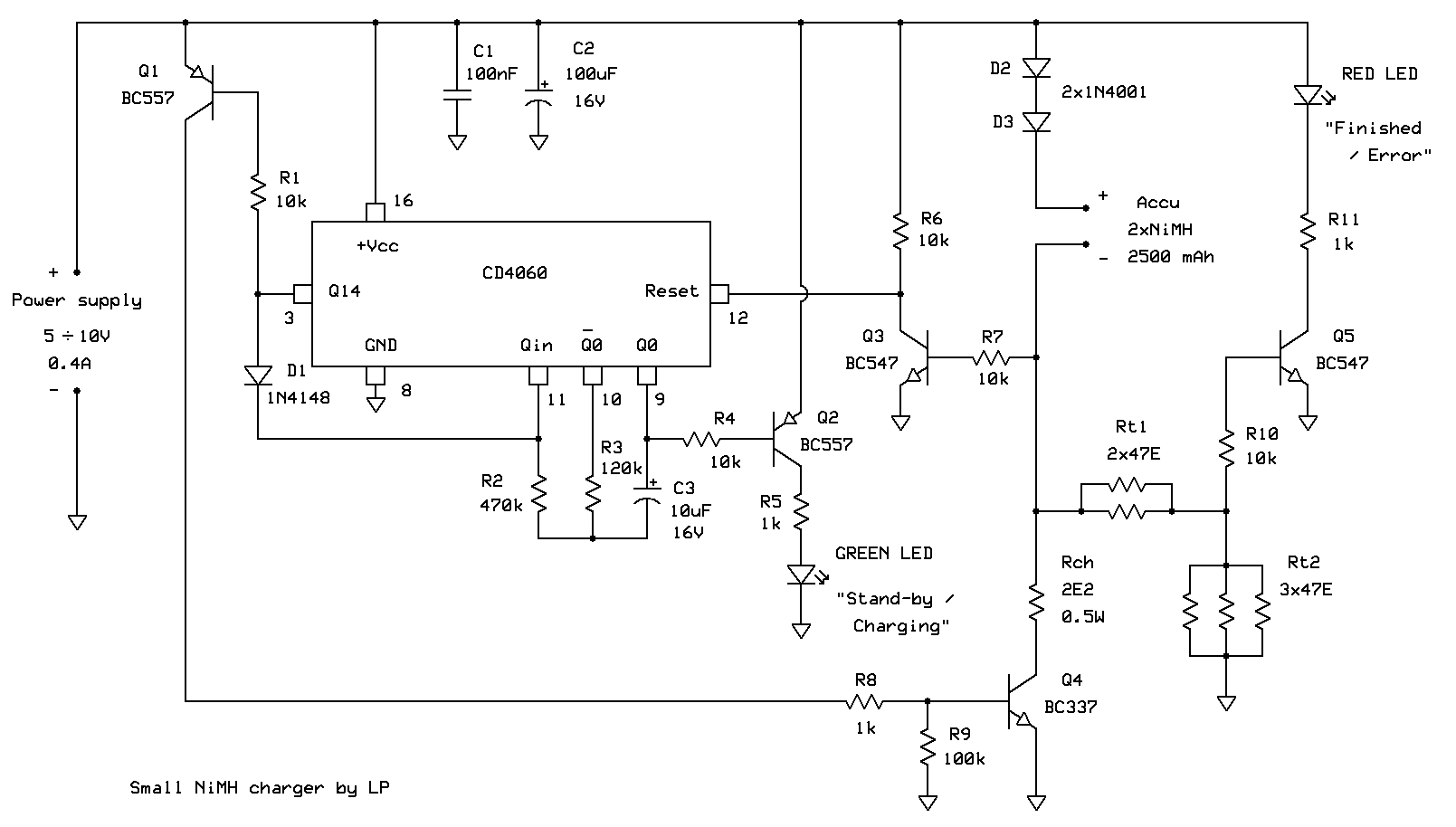
This charger is expected to be custom built for a particular cell (or a pair of cells), meaning that it is best to measure the capacity of the actual cell(s) that will be charged by it and then calculate the amount of time necessary for charging them using the current capability of the power source one picked, before building the circuit. There are special ICs on the market that implement more advanced charging methods, for example U2402B that uses “multiple gradient” technique, able to precisely recognize the moment when cells being recharged become 100% charged and then stop further overcharging, without prior knowledge of remaining cell charge, capacity, temperature etc. But a simple timer is often all one needs to prevent overcharging the cells if their capacity and nominal output current of the charger are known. It is not advisable to build fast chargers this way, but if charging interval of a few hours suffices, then this little circuit will suit one’s needs nicely.

As can be seen, the core component is a CD4060 timer. This inexpensive IC contains an RC oscillator able to generate very wide range of frequencies (Hz to almost MHz) and a 14-stage binary counter that extends the basic oscillator time interval up to 2^14 = 16384 times. If for example the oscillator output Q0 flips its output every second, Q14 output will change its logic state once every 4 and a half hours! This wide range of available timed intervals serves dual purpose here - both to turn off the charging current after a few hours, and also to blink a pair of LEDs that indicate the charging phase.
The operation of the device is easiest to understand if we assume that accumulator is connected to + and - charging ports (+ pole of the cell goes to + port) and that the charging is in progress. If so, IC counts intervals of approximately 1 second each, so that Q0 output uses transistor Q1 to alternatively turn green LED on and off. The only two components that set the time interval are R3 and C3. The formula that calculates the oscillator frequency is:
fosc = 1 / (2.2 * R3 * C3) .
where each complete oscillation interval consists of one half-interval in which Q0 is in logic low, and the ather half-interval in which it is in logic high state. Therefore, if R3 = 120kOhm and C3 = 10uF, Q0 is alternatively logic low and then logic high for approximately 1.1 * R3 * C3 = 1.33 seconds each. For the purpose of oscillator stability, R2 should be at least 3 times higher that R3, while R4 can be as low as 10k since Q0 output current capability is higher than 5V/10kOhm = 0.5mA.
If the end of charging is not reached, Q14 is logic low and consequently PNP transistor Q1 is turned on. This means that transistor Q2 is also turned on and that charging current is flowing through Rch and the cells. Q2 should be powerful enough to withstand the full charging current for several hours, and that is the reason that BC337 is selected (Imax = 800mA). Rch sets the charging current according to the next formula:
Ich = (Vcc - 2Vbe - Vaccu) / Rch .
where Vbe = 0.65V is voltage drop on two diodes D2 and D3, and Vaccu is accumulator voltage (approximately 1,4V per cell while recharging). With component values as denoted in the diagram, we get: Ich = (5 - 1.3 - 2.8)V / 2.2Ohm = 0.4A . Power dissipation on Rch is easy to estimate: Pch = Ich^2 * Rch = 0.4 * 0.4 * 2.2 = 0.35W. One should pick a bit stronger resistor than that, i.e. at least 0.5W one in this case.
While charging, green LED flipps on and off every 1.33 seconds, while voltage drop on Rch is Vch = Ich * Rch = 0.4A * 2.2Ohm = 0.88V. Voltage at the point in which Rt1 meets Rt2 is only 0.88V * (Rt2 / (Rt2 + Rt1)) = 0.35V, and the same voltage can be found at transistor Q5 base meaning that it is turned off. This of course means that red LED is also off.
After IC counts (2^14)/ 2 = 2^13 = 8192 basic Q0 time intervals, Q14 output changes its state to logic high (because it reached 1/2 of its own time interval). This happens after 2.2 * 120k * 10uF * 8192 = 6.00 hours have elapsed. At that moment diode D1 pulls Qin oscillator input to logic high preventing further oscillations, effectively stopping the timer permanently without resetting it. Because of logic high Q14output, transistors Q1 and Q4 turn off. This means that charging current cannot flow through Rch anymore, and the only remaining charging current now goes through Rt1 and Rt2. This “top-off” charging current is: It = (Vcc’ - 2Vbe - Vaccu) / (Rt1 + Rt2) = (8 - 1.33 - 2.8)V / 39Ohm = 100mA, or merely 4% of the nominal cell capacity (note that Vcc’ is now 8V because the unstabilised AC/DC adapter output current has dropped significantly). Since NiMH cells are produced so that they can withstand overcharging currents up to 10% of the nominal capacity (i.e. up to 250mA if the nominal capacity is 2500mA), this cannot damage the cells. It is of course not advisable to leave the cells in this charger indefinitely, but keeping them in for several additional hours after the main charging phase is finished will not do any harm.
After the oscillator is stopped via D2, its Q0 output goes logic low which turns off the green LED. At the same time, voltage drop on Rt1 + Rt2 resistors is now (8 - 1.33 - 2.8) / (Rt1 + Rt2) = 3.9V, meaning that voltage at their meeting point is 3.9V * (Rt2 / (Rt1 + Rt2)) = 1.55V, which is more than enough to turn Q5 and red LED firmly on. Note that in case of stabilized power supply voltage, such as USB +5.0V, the previous technique would not work.
Thus far, the two phases of regular charging process have been explained. But careful readers observed that both LEDs have dual designations in the diagram. Here are the reasons. If there is no accumulator connected to the terminals, Q3 base is via Rt1 and Rt2 pulled to 0V. This lets R6 pull Reset input of the IC to +Vcc, which keeps it in a reset state. Oscillator is not running, but Q0 output is logic high which means that Q2 and green LEDs are turned constantly on. Hence the “Stand-by” marking. Note that the charger resets itself this way every time the cells are pulled out from the housing, which means that after the first set of cells is recharged and pulled out by the user, it is instantly ready to begin charging another set of cells.
If the user erroneously plugged in cells with reverse polarity (cell + pole to charger - terminal and vice versa), nothing bad should happen. Most importantly, even if power supply is not connected (AC/DC adapter not yet plugged into the wall outlet), both adapter and IC cannot be damaged by reverse voltage due to protective action of D2 and D3 that prevent the reverse current flow (a single diode is enough for this, the two of them are used here only to control red LED operation based on Rch/Rt voltages as described earlier). If the power supply is connected, then direct current will flow through accumulator cells, D2, D3, Rt1 and Rt2. In this case, accumulator voltage is added to the power supply voltage, so the approximate current is: Ierror = (8V - 1.33V + 2.4V) / (Rt1 + Rt2) = 0.25A. Power dissipation on Rt2 component resistors is then 0.25A^2 * (47 Ohm / 3) = 1W => 0.33W on each Rt2 third, while power dissipation on Rt1 component resistors is 0.25A^2 * (47 Ohm / 2) = 1.5W => 0.75W on each Rt1 half. This is way too much heat if one used 1/4W components, but observe that in this case voltage at Rt1/Rt2 meeting point is now 3.9V which turns red LED on. Therefore, the user is instantly and undoubtedly warned about the erroneous cell insertion. If one wonders whether such obvious mistakes ever happen in reality - of course they do! It’s not only the usual inverse of user intelligence to blame, but also external factors such as too high level of ethanol in blood after brutal partying (in which taking too many photos for the Facebook took place so camera batteries needed recharging) or severe sleep deprivation caused by exhaustive work on an embedded programming project (that eventually got interrupted in early morning hours only by the discharged wireless keyboard), and so on...

