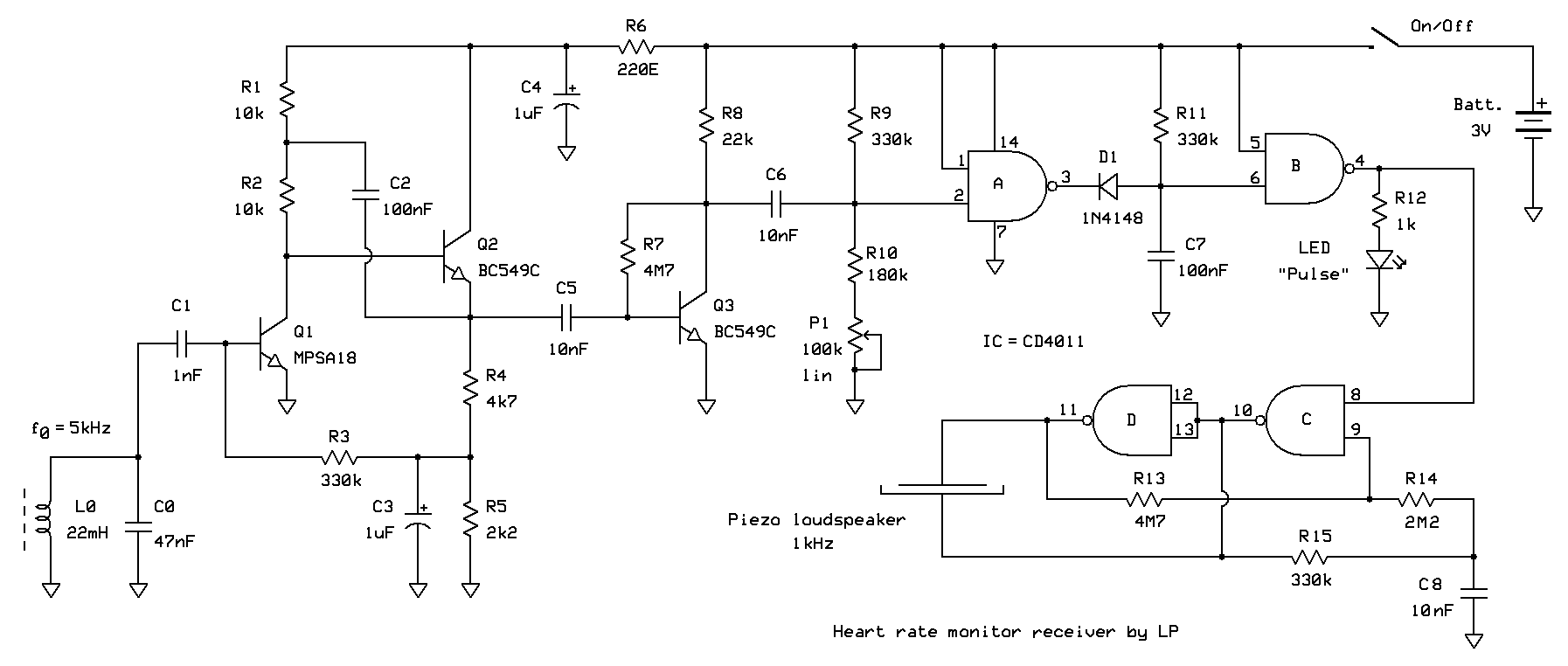
Receiver circuit
So we need a circuit that responds to short pulses of electromagnetic energy at 5kHz carrier frequency, with the sensitivity set reasonably high so that it will be able to discern low power pulses from the noise, and then we need a means to indicate detected pulses to the user. In reality this turned out not to be a particularly hard task. We opted for a simple and very well behaved two stage bipolar transistor preamplifier and signal shaper/indicator made out of a single digital IC. Parallel resonant LC circuit in the front end serves a dual purpose - it selects carrier signal from the electromagnetic spectrum while its inductance L wound onto a small ferromagnetic core also acts as a handy and robust antenna.

Q1 and Q2 and surrounding components form a directly coupled AF amplifier with a few very useful features, the most prominent one being the possibility to set collector currents of both Q1 and Q2 to stable, precise and rather low values. If Vcc is constant, Q1 collector current Iq1 depends solely on values of R1 and R2:
Iq1 = (Vcc - (2*Vbe)) / (R1 + R2) = (3 - 1.2) / 20k = 90 uA .
Keeping it low is important for three reasons:
-
We don’t want to drain the battery too much
-
Q1 collector current dictates its noise factor (NF) i.e. receiver sensitivity and
-
Q1 input impedance is reasonably high only if its collector current is low.
Having all this in mind, we decided that 90uA is a good compromise for Q1 current. It gives input resistance of approximately:
Ri = (Vt / Iq1) * B1 = (25mV / 90uA) * 900 = 370kOhm
which is high enough so that resonant L0C0 circuit will not be loaded too much. This is favorable because the passband of an unloaded LC circuit is very narrow, which leads to not only high amplification of tiny pulses due to resonant circulation of energy inside it but also to high rejection of out-of-band signals, both factors contributing significantly to receiver performance.
Q1 is a special (but inexpensive and easy to find) so called “super beta” low noise transistor. It is designed so that it generates low internal noise voltage and currents, while a the same time having very high amplification of externally fed signals. On can also use BC549C or similar relatively low noise NPN transistor for Q1 with similar results (usable range of the receiver). In the circuit above Q2 is added to Q1 as a “bootstrap” follower, the purpose of which is not to amplify signal voltage by itself, but rather to make a more favorable electrical environment for Q1 operation. It does so by effectively turning resistor R2 into an alternating current source by keeping the signal voltage between the two ends of R2 constant using the positive feedback component C2. If one remembers that voltage amplification of a bipolar transistor with the grounded emitter is proportional to the ratio of its collector- versus emitter impedance, it is not hard to conclude that Q1 voltage amplification is in the order of thousands!
One could argue that Q1 and Q2 put into this particular configuration produce very similar net amplification as if two simple separate concatenated amplifier stages (such as is the one with Q3) built out of Q1 and Q2 would have, each contributing to the amplification by a factor of around one hundred i.e. 40dB. This is of course true, but one should note that Q1/Q2 bootstrapped amplifier is much more linear and in terms of temperature variations more stable circuit. It appears that good engineering habits, not only the bad ones, are hard to let go so we opted for the circuit as presented here :)
Another objection can be made with regard to very high Q1 voltage gain. A well known fact is that designing the first stage of a low noise preamplifier so that it has high gain is not a common practice especially in radio community as it easily leads to unnecessary distortion and intermodulation problems in receivers, but in this particular case, in which all we need to do is to detect the presence of an uncoded signal pulse, that is luckily of no concern.
If signal voltage amplitude generated inside L1 is in the uV range, then Q2 output is somewhere in the mV range. This is still too low to be processed directly by digital circuits, so we tossed in a simple AF amplifier stage built around Q3. So finally at Q3 collector we are talking volts. The rest of the circuit is a simple mono stable multivibrator where gate A does the triggering, while gate B once triggered (C7 discharged) keeps LED lit for a fraction of a second. In contrast to most circuits presented at this web site, we did not want to use ICs with Schmidt inputs here - although it seems that it would have made the receiver more noble, it would instead render it rather deaf as it would then require pretty high input signals in order to power up the LED.
Instead of simple LED blinking, noise-free gate B output signal can be fed into a microcontroller or a PC and then processed further as desired. For example, it would be easy to record heart rate over time and use that information for asessing athlete's performance after the test. Just remember to reserve enough digital memory in advance and to prevent high frequency digital noise from entering the receiver from the "back side" - inserting an optocoupler between gate B output and digital signal processor input can help if that becomes an issue.
Two unused gates can be put into good use by turning them into a beep oscillator as is depicted in the circuit diagram. Gate D together with resistors R13 and R14 turns gate C into a Schmidt-input inverter, which is then used in a standard astable multivibrator circuit in order to generate audio frequency tone. A small resonant Piezo loudspeaker is connected to outputs of both inverters in order to produce a bit louder sound than if it were connected to ground.
There is however an unusual quirk of this particular receiver - since it is sensitive to frequencies of a few kHz, and since tones one usually generates for beeps are of the same sort, it is fairly easy to make the receiver jamming itself with audio beeps it generates. It may seem funny, but after a respective amount of fiddling with the components layout, we concluded that it is actually more convenient to simply leave out the beep generator out of the circuit altogether and be satisfied with nice and harmless LED blinks!
None of the components is critical so the design can easily be reproduced by even less experienced electronic lovers. The only two components the values of which should not be changed are L0 and C0 as they set the resonant frequency of the receiver. Sensitivity of the prototype is approximately 1m (3 feet) and is comparable to the sensitivity of the dedicated factory made receiver inside the watch that came with the transmitter. In our prototype, L0 was a standard ready made inductor formed onto a tiny ferrite core.
If longer range is desired, L0 can be hand made using an old medium wave ferrite antenna with a certain number of turns of enamel wire wound onto it. Such “antenna” would almost certainly be several times more sensitive than the one we used, but one should be a bit cautious with it - it turned out that although the receiver is tuned to 5kHz, in a common house nowadays there seems to exist such huge amount of electrical noise that it can jam the "too sensitive" receiver. Don’t be surprised if the receiver becomes stirred up near TV sets, mobile phone chargers, PCs and other household appliances because as the time goes by more and more of them contain switch mode power supplies that generate a lot of electrical noise in kHz to MHz range. The most promissing cure to this issue lies in digital signal processing domain, which is out of the scope of this article.

