Complete circuit diagram
The first glimpse at a circuit reveals that there isn't anything spectacularly new in it. It can be easily divided into two main building blocks: 1) preamplifier built with Q1, Q2 and surrounding components, and 2) output power amplifier. But there is in fact quite a bit that can be said about this device as it is very finely tuned to be up to the task - both in terms of detailed topology and component values used. On this page and the next one, we will dwelve rather deeply into details of this handy circuit. Hobby designers intrigued by analog circuit design will be able to add a few more tricks up to their sleeve after reading the rest of the text.

Note
Although the circuit topology itself provides rock solid performance in terms of combating wide component value tollerances, temperature changes and power supply voltage drifts, most resistors and practically all capacitors should have exact values as shown on the above diagram in order to match frequency band requirements posed by the purpose of the circuit. Contrary to most other circuits presented on this website, readers are advised not to change component values much. But then again, what's the point of making an experimental circuit if one doesn't play a bit with it?
Preamplifier
Stethoscope preamplifier must have a relatively high gain which implies that it also has to be of very low noise. In addition, since lowest frequency audio signals incomming from the microphone can occasionally have pretty high amplitudes, the preamplifier must also have as large dynamic range as possible in order to avoid saturation and clipping. Directly coupled two stage amplifier circuit topology enables all of that plus offers several other significant advantages compared to more "traditional" AC coupled preamplifiers. Read on.
DC currents of both transistors are very stable and can be easily tailored to suit the design requirements. More on what this exactly means a moment later. Stability comes from a very strong negative DC feedback formed by connecting Q1 base resistor (220 kΩ) to Q2 emittor resistor (2k2). Any temperature or power supply voltage instability reflects as voltage change at this point influencing collector currents of Q1 and Q2 in such a way so that they tend to return to their ideal values. For example, should Q2 collector current increase, voltage drop over 2k2 resistor would increase too, so base polarisation voltage of Q1 would also increase. That would lead to increase in Q1 collector current. This additional current could not be provided for Q1 from anywhere else other than Q2 base current, so this leads to Q2 base current being decreased. This naturally decreases Q2 collector current which in turn decreases voltage drop over 2k2 Q2 emittor resistor. Hence perfectly stable DC performance. Note that Q1 controls Q2 collector current so that it is always given simply as: Vbe / Re, which in this case is: 0.6V / 2k2 = 0.27 mA.
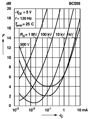
As for choosing Q1 collector current, it is solely dictated by optimising its noise performance. For each bipolar transistor type, there is an optimal collector current value for which the component exibits the lowest possible noise when its input signal is provided by a generator with certain internal resistance. For transistors intended to be used as small signal preamplifiers, optimal currents are sometimes given in manufacturer datasheets, as is the case for BC559 series transistors. In this particular circuit, signal generator internal resistance is practically equal to the value of the microphone polarising resistor. As can be read from the diagram silently stolen from BC559 datasheet (note the erroneous units designation of signal generator resistances used as parameters), an optimal Q1 current is then approximately 0.02 mA in which case it introduces some 0.7 dB of noise. This is really not bad at all.
Calculating Q1 collector current is extremely simple too, simpler even than in case of AC coupled preamplifiers. Surprisingly, Q1 collector current depends solely on its collector resistance, which at the same time serves as Q2 base resistance. In this case, it is a series connection of two 27 kΩ resistors. Note that DC voltage drop over this resistance is constant if power supply voltage is constant and it is precisely: Vcc - (2 x Vbe) - V3, where Vbe is base polarisation voltage, tippycally 0.6V, and V3 is voltage drop over 10 kΩ resistor connected between 2k2 and Q2 emitter. Can you figure out why this is so? What we need to do is to find DC voltage at Q2 base with respect to GND. Obviously, that voltage is 0.6V lower than Q2 emitter voltage. So then, what is Q2 emitter voltage? That's easy - if we rightfully neglect voltage drop over 220 kΩ Q1 base resistor, we can conclude that voltage drop over 2k2 resistor must be equal to Q1 base voltage, for which we know is precisely Vbe = 0.6V for all silicon bipolar transistors. So Q2 emitter voltage is then equal to the sum of voltage drops over 2k2 and 10 kΩ resistors. Since the same Q2 emitter current flows through both these resitors, then voltage drop over 10 kΩ is given as: V3 = (10k / 2k2) * 0.6V = 2.7V. Now we are ready to execute numerical substitutions and find that Q1 collector voltage with respect to GND is: 9V - (1.2V) - 2.7V = 5.1V. If this is so, then Q1 collector current is given as: IcQ1 = 5.1V / 54 kΩ = 0,095 mA. Note that unlike in AC coupled amplifiers,
Q1 collector current doesn't at all depend on its base resistor. This means that we can pick unusually low Q1 base resistance considering its collector current, which is a huge advantage of this topology over usual AC coupled single transistor stages when designing low noise preamplifiers since high ohmic resistances are the prime cause of noise generated inside amplifiers. In this particular example, Q1 base resistor has a handy value which enables easy filtering out of unwanted high frequency audio components above approximately 1.2 kHz using tiny 13.3 nF plastic cappacitor.
Let's now move slowly to Q2. A careful reader might ask themselves why Q2 is connected in common collector configuration as its voltage gain is then equal to 1. What's the purpose of using a two-stage preamplifier if one of the stages doesn't amplify the signal? Well, this is of course not quite so. Observe a 10 �F cappacitor connected between Q2 emitter and Q1 collector resistance mid-point. Does this ring a bell? A more experienced readers will recall that this is a so called "bootstrap" circuit. Bootstrapping is term used in electronics when we want to emphasise that a circuit is configured so that a component basically "drives itself". This is of course not literally possible but instead usually means that a very strong negative feedback is formed around it so that its surrounding imedances (in this case Q2 base resistance) are significantly altered in AC domain compared to DC domain. If we remember that cappacitor voltage cannot be changed instantly, then we can observe that 10uF capacitor practically translates AC voltage signals from Q2 emitter to Q2 base resistance mid point. This in turn means that
voltage drop over the upper 27 kΩ resistor is constant - it doesn't change at all during the circuit AC operation. And if voltage drop over a constant resistor is constant, that means that the current flowing through it is constant too - it behaves as a
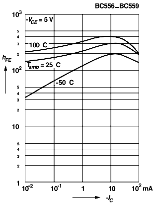
constant current source. Equivalent Q1 collector resistance in AC domain is therefore much much higher than 27 kΩ and in an ideal circuit it would be infinitely high. Why is this important? Because voltage signal gain in common emitter configuration depends strongly on collector resistance - the higher the resistance the higher the gain. So, although Q2 doesn't amplify AC signals directly on its own, what it does is providing ideal conditions for Q1 to give its best. Thanks to Q2 bootstrapping action, Q1 amplifies input AC signals not a merely 150 times as the diagram on the right suggests, but instead thousands of times! And don't forget: the higher the collector resistance, the higher the amplifier linearity.
Exact DC operating point of Q2 is easy to calculate. In order to enable as wide signal dynamic range at the output of the preamplifier as possible, Q2 emitter DC voltage shoud be approximately Vcc/2. Since we already know that voltage drop over 2k2 resistor is precisely 0.6V and that consequently Q2 collector current is 0.27 mA, it is not hard to calculate that additional Q2 emitter resistance should be roughly 15 kΩ. Note that Q2 emitter current and followingly collective voltage drop over the series connection of 2k2 + the_additional_resistance doesn't depend on Vcc, so in order to provide some margin for preserving wide dynamic range when battery voltage drops below its nominal value, we should pick a somewhat lower value for the additional emitter resistance. 10 kΩ seems to be a good compromise.
The reason that PNP bipolar transistors are used in the preamplifier is that under same conditions they generate about 30% less internal noise compared to their NPN equivalents. This is a general rule. Simply put, noise that we observe originates in random thermal jitters of electricity carriers inside electronic components. Majority carriers in NPN transistors are electrons while in their PNP counterparts those are so called "holes" i.e. electron voids inside a crystal lattice. Holes are therefore "missing electrons" which may be imagined as virtual positive particles moving around the semiconductor crystal lattice in similar fashion to electrons, but in opposite directions. They have positive charges equal in absolute value to electron negative charges, but for some reasons they appear somewhat more massive than electrons. This leads to their lower motility. From the standpoint of useful electrical signals generated by surrounding components, there is practically no difference in transistor operation whether it uses electrons (NPN type) or holes (PNP type). But since holes are less motile, they don't fly around the lattice in random fashion due to thermal energy that much as electrons do. A positive consequence is that PNP transistors always appear to be less noisy than NPN ones. The drawback is that PNP also have lower maximal operating frequencies than NPN equivalents, which is of course of no concern in audio signal amplification.
To conclude this long page, the preamplifier topology presented here enables optimal and easy to implement Q1 and Q2 current setting according to desired noise performance while at the same time it provides very high small signal gain, wide dynamic range, excellent linearity and absolute DC stability. What more could a happy designer wish for :)